Rino Micheloni is a well-known storage and memory technologist and author. He is currently a Fellow at Microsemi Corporation in Italy. Rino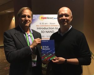 has helped me with the Flash Memory Summit many times over the years (note the sign in the background in our picture to the right).
I was very happy and honored last year when Rino asked me to write the foreword to his latest textbook: 3D Flash Memories. This up-to-date volume was published earlier in 2016 by Springer.
Rino and his publisher have kindly agreed to let me share that foreword in this post.
“In 1903, the Wright brothers made the first powered flight into the third dimension. After fulfillment of this ancient dream, predictions of longer, faster, and safer flights were easy to make. Fundamental, practical breakthroughs, such as this first powered flight, are momentous when achieved. But even more striking are the unforeseen achievements that these breakthroughs enable and inspire. Few would have predicted that humans would leave footprints on the surface of the moon only 66 years after the Wright brothers’ first flight.
The semiconductor industry touches nearly all parts of our lives and quietly scales precision manufacturing to volumes unimaginable with other methods. Wafers of nonvolatile memory (NVM) routinely are fabricated with trillions of individual cells. Although challenging, this density of components was predictable from the early days of Gordon Moore’s observations that the number of components on a 2D integrated circuit would double every year, and later every 2 years (“Moore’s Law”[1]). Harder to predict, in 1965, were the inventions of the internet, smart phones, and autonomous vehicles. These are economically possible largely because of Moore’s Law.
The doubling of components is slowing to every 2 ½ years.[2] But we have also arrived at an unprecedented inflection point for Moore’s Law. Component density can continue to increase by building into the third dimension. Other technologies have already added an “extra” dimension. These include pressure-sensitive touchscreens, video gesture capture, autonomous vehicle navigation, 3D printing, and drones that maneuver throughout the sky.
Traditional 2D semiconductor processing obviously includes the third dimension. Material thicknesses are varied; devices are formed by multiple layers of materials and shapes; and interlayer interconnects enable complex routing. Furthermore, “FinFET”[3] 3-dimensional transistors have been shipping in microprocessors for several years. However, the processing that is currently utilized for 3D (or “vertical”) NAND flash is fundamentally different. 2D processes fabricate devices that can be fully enumerated by viewing the x–y plane of the wafer from above. However, 3D flash also fabricates devices that are enumerated in the z direction, perpendicular to the plane of the wafer. Just as in 1965 when Gordon Moore published his projections for the future of semiconductor fabrication, we cannot foresee all of the benefits that scaling in this additional dimension will provide.
It would be shortsighted to dismiss 3D semiconductor processing as just an incremental step in the progression of micro/nano-electronic fabrication. This new dimension multiplies the number of elements that can be created with the same number of photolithographic steps. As experience in manufacturing is gained, this multiplier grows from dozens, to hundreds, and possibly beyond. Fabricating devices in the third dimension provides a new degree of freedom for creativity in designs, architectures, and layouts. It offers challenges to create breakthroughs in testing, integration, power density, heat dissipation, and systems-on-chip. 3D semiconductors can become a profitable platform for experimenting with interactions between these fields to yield new economies of scale that do not yet exist.
3D upon 3D systems are being imagined in which a stack of varied devices can replace a computer, and eventually a portion of a data center. What is not yet seen is the new field of view these advances will clear so that we can envision what is beyond them. Becoming efficient at building 3D flash is likely to be a critical step on the path to creating what has not yet been imagined. It is often said that what used to take a roomful of electronics now easily fits in our pockets. 3D processing may allow us to make the same statement about a roomful of today’s technology. It may also allow us to say that what once took a pocketful of components now fits in a blood cell.
To accelerate the implementation and adoption of 3D systems, clear, practical information is needed. Rino Micheloni’s new book provides a wealth of hard-to-find information that can help push the industry forward. It can expand the number of people who confidently take the first steps into new manufacturing possibilities. Just as the practical skills needed for creating powered flight were learned in a bicycle shop, the practical skills for creating the next breakthroughs of nano-electrical systems are being learned in 3D flash fabs. This large industry will serve as an invaluable incubator from which future jobs, employees, and inventors will grow.
University professors are encouraged to build on the information in this book and make 3D complexity clear and understandable for the next generations of graduates. 3D processing and design will likely move from the “future topics” section of classes to core fundamentals of the engineering curriculum. Students will learn how to efficiently transport charge at the three dimensional nanoscale and perhaps have routine undergraduate lab exercises on the manipulation of electron spin from one layer to the next.
The important lessons learned by fabricating 3D flash in high volume will provide insights for forming nanoscale “vertical” structures that can act as scaffolding for future manufacturing techniques. These scaffolds might support and direct self-assembling structures or even biological growth. Such structures and know-how may revolutionize power efficiency, health care, and system miniaturization.
As cost and power efficiencies are realized, products with tremendous processing, sensing, and data densities can be expected. These products may make it possible to automate and optimize tasks from the critical to the mundane to the joyous. Affordable weather forecasts for your precise location may become available. Autonomous transport will free up many human hours lost while driving, enabling an increase in personal productivity. Ever more capable personal assistants will provide custom coaching for your athletic performance, artistic expression, or even social interactions.
This high density of processing, sensing, and data will enable early-adopters to differentiate their products and services in new ways, creating profitable market opportunities. As 3D processing becomes more commonplace, its techniques may be applied to existing products to improve their utility, cost, and power consumption. Optimal design, across all electronics, might need to be redefined. We are likely to see old industries disrupted and new ones created.
Thank you to Rino and his many authors, contributors, supporters, editors, and staff for creating an accessible source of difficult-to-obtain knowledge on 3D memory. I believe your work will serve as a catalyst for accelerating advances in 3D wafer fabrication. This, in turn, will accelerate advances in the many fields that depend on semiconductor technology.
Charles H. Sobey
Plano, Texas, USA
2015[1] G. Moore, “Cramming more components onto integrated circuits”, Electronics Magazine 19 pp.24-27, (1965); Additional information at: http://www.computerhistory.org/semiconductor/timeline/1965-Moore.html
[2] Recently, Intel has stated that since the 22nm process node two and a half years is the pace of doubling of components per integrated circuit: http://www.cnet.com/news/keeping-up-with-moores-law-proves-difficult-for-intel/
[3] C. H. Lee et al., “Novel body tied FinFET cell array transistor DRAM with negative word line operation for sub 60 nm technology and beyond”, VLSI Technical Digest, pp.130-131, (2004)”